
Industrial Print was originally defined as when print was applied to manufactured products, such as a logo on a washing machine or informaiotn on the packaging. In this format print usually conveys information, identifies brands and communicates motivation to buy the product in some combination. But it can also include print for the sake of decoration on its own, as say, on building materials. It has now even come to include patterning and deposition of functional materials on or in manufactured products, think printed circuit boards, and their successors, printed transistors.
In all these applications the overriding characteristic of industrial print is that it is a sub-process in manufacturing – a kind of product component. That has important implications for the performance parameters of print processes, which must be subordinated to often extreme manufacturing parameters. Think of flexible meat packaging proceeding from plastic granules through multiple laminations of functional material passing through extremes of moisture and temperature having to be printed somewhere along the way before the meat is packed and pallet-ready for dispatch to retail at the back door of the factory.
When print is applied to manufactured products generally a lot more is asked of it than in the document printing world. It has usually to be of a high quality often exceeding document standards, especially on miniaturised surfaces, must be able to be applied economically to shapes, forms and surfaces which are not optimised and are sometimes outright unfriendly for print, and it has to be supremely durable on products that long outlast their communications‘ lives at retail.
Because of the unusual diversity and complexity of the surfaces that must be printed in the industrial sectors, and because of the conditions to which print is subjected during and after manufacture of products, industrial print often calls for relatively specialised print (and pre/postprint) processes. There are no simple rules about this and ordinary document print processes like offset and gravure are often used where they can be as they bring low cost and high quality. But many times in industrial sectors rough, thin and rigid surfaces dictate the need for flexo printing where a flexible image carrier plate can conform to the surface, think metal plates, or thin flexible films in packaging or an embossed decorative panel, or textiles which require screen rollers to push large quantities of ink into its absorbent weft. Industrial applications require chemical resistances, high opacity and dense layering that can sometimes vary from a few to several hundred microns. This represents a higher level of chemistry as the ink must withstand high temperatures, it must meet high standard and quality controls whilst being durable over time.
Depreciation of ink quality is not tolerated within industrial print processes. Sometimes too the substrate is in a macro sense three-dimensional, or curved like a metal part. That can call for screen printing or even pad printing for severe curvature – think a rounded product edge or handle/knob/button – where say a screen image carrier can be customised to the surface or allows extreme flexibility (silicon pad for example). If you have to print a relatively small number of a very large surface in one go that can also be appropriate for screen printing which is capable of large sizes without dictating large run length economics. Choice of print technology is sometimes an economic choice. In general in industrial print markets you find that shorter run jobs make up a bigger share of overall print volume within the fragmented structure of such a diverse marketplace than you will in say document printing. This translates to relatively high print costs, and relatively high print margins.
Both ways of looking at this suggest opportunity for enhanced technology offerings like digital print. Due to the low surface energy of many industrial market substrate surfaces you find in these markets a more common application of solvent ink chemistry than elsewhere. In addition to low surface energy of the substrate, speciality ink chemistry is needed for applications such as ceramics, but also in addition, printing onto plastics with solvent, two component solvent and UV-Curable printing processes. It should be noted that for best production performance, UV technology is the process of choice for specific needs. Screen printing remains a mainstream print technology in the industrial sector, and not only in functional, smart screen printing and can include decorative, direct print onto packaging containers, membrane switches, IMD parts and photovoltaic print.
The German VDMA Printing and Paper Technology Association looks into major players of this market. Professor Dr Reinhard Baumann, university professor at TU Chemnitz and coordinator of the Go Beyond 4.0 lead project at Fraunhofer-Institut ENAS for electronic nanosystems in Chemnitz, talks about trends and printing methods applied in printed electronics, as well as about what functional printing can perform beyond Industry 4.0.
The Fraunhofer ENAS and TU Chemnitz are also members of the VDMA Working Group OE-A (Organic and Printed Electronics Association), which is in close contact with the Association Printing and Paper Technology.
Industrial printing is cited by suppliers, associations, researches and analysts as a major growth area and opportunity.
Prof Baumann, how do you define Industrial Printing?
PB: It is first of all the mass production of print products for different markets. The existing print technical knowledge can be used for products and markets beyond traditional printing. Previously it
mainly addressed human vision and partly also touch and smell.
This is still true as far as decorative, textile and packaging printing is concerned. However, there are also new applications that cannot be perceived by human senses. As a result, printed electronics give access to very interesting markets. Yet it is still open who will serve them.
Which printed functionalities are in the focus at Fraunhofer ENAS?
PB: Our aim is to print defined patterns of materials on preferably flexible substrates using any kind of liquids. These patterns must satisfy highest demands as to precision and layer thickness without any need for post-processing. For printing, silver and other, often very expensive conductor and semi-conductor materials based on nanoparticles are used. In addition, UV inks as insulators are also used.
Conductors, semi-conductors and insulators are the basic components of electronics. They can be used to produce printed circuit boards with resistors, diodes and transistors, but also batteries and antennas.
The advantage: Material is only deposited where it is really needed. Compared with etching and laser processes, the amount of material used, the processing time and the expenditure for production as well as recycling are lower. In addition, vacuum or clean room conditions are not required for printing.
Nevertheless, the efficiency level in transistor printing is more than 90 percent.
We have printed ten thousands of them, have continuously improved the parameters and geometries and have found out: The smaller the transistors, the more reliable the process.
Here, it is not about highly complex microchips, but there are definitely applications.
Which ones?
PB: Printed sensor networks in which we print large-area sensors. Or individually designed, environmentally friendly zinc manganese dioxide batteries. We can scale their energy contents and design them for the respective application.
Our antennas are geared to the ultra-high frequency (UHF) range – for instance, for RFID labels and even higher communication frequencies.
The use of RFID in logistics was rather weak because the labels produced in large quantities worked only partially. This was often due to the dielectric environment. We adjust the shape of the antenna to the specific application and thus achieve a highly reliable communication.
The RFID technology functions consistently good when we work on a three-dimensional basis, for instance, by printing antennas on the folding edges of a package.
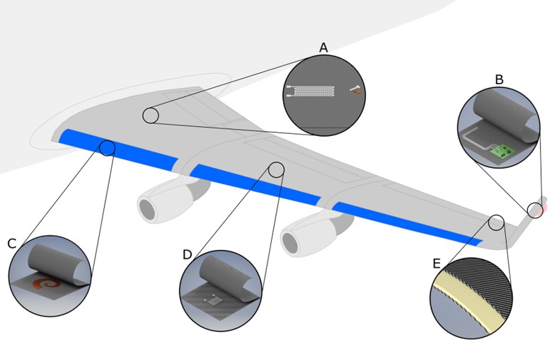
We also develop printed functions for the interior and exterior of cars and aeroplanes. Furthermore, there are other interesting markets: The lab-on-chip technology for which we print membranes using inkjet processes and where we can exactly scale their pore sizes.
Do you use traditional printing methods or rather digital methods?
PB: We use both traditional and digital to research industrial printing.
On the one hand, we use the screen and gravure printing processes with which we, inter alia, produce homogeneous, precise layer thicknesses in fuel cells.
Gravure printing is also the process of choice for high-resolution patterns thanks to its inherent process.
However, we above all use digital inkjet methods, since they enable us to process a huge variety of inks.
We have inkjet heads that apply nearly every liquid.
Considering the high price of inks, it is important to minimise the ink volumes in the inking system.
To which extent do the workflow and the associated measurement technology change?
PB: When you look at the process from the data source to the end product, it is a production technology like any other. Here, the printing machine is just one of a large number of output systems.
Quality inspection, however, is demanding. Vision inspection methods ensure production only to a limited extent. Other measurement methods are, for example, required when ceramic inks with piezoelectric properties are used.
This opens up an important field of research which will be crucial for the broader application of functional printing.
Do you see your research as part of printing technology or rather of microelectronics?
PB: I see it as a general production technology within the scope of which we use printing technology in order to integrate innovative functions into products.
What we understand by it can be explained by looking at the Go Beyond 4.0 Fraunhofer lead project, which I am coordinating, as an example.
We explore the application of printing methods for wireless touch functions in the interior of automobiles, the printing of sensors directly onto fibre composites, for instance, on aeroplane wings as well as individualised lighting systems.
Our aim is to manufacture products from quantity one in networked process chains. Digital functional printing is optimally suited for individualisation in mass production.
The digital printing method converts data directly into functions which are then deposited in the production line exactly where a customer needs them.
Furthermore at lower cost, with less usage of material and utmost reliability. This approach goes far beyond Industry 4.0 and will work in different industries. Together with a partner company in Chemnitz, we develop the modular machines that are needed for that.
Market studies predict a strong global growth for industrial printing. Where do you see the most important growth sectors – from today`s perspective?
PB: The supporting industries are the automotive industry which needs new energy storage systems for electromobility and new engineering concepts for self-propelled vehicles, the aerospace industry as well as the microelectronics and lighting sectors with interesting niches for functional printing.
Comment below to have your say on this story.
If you have a news story or tip-off, get in touch at editorial@sprinter.com.au.
Sign up to the Sprinter newsletter